About
New glorious technology comes to your modular system! With this device, one can recall vast entire six states, each recalling as many as three controls! Order now!
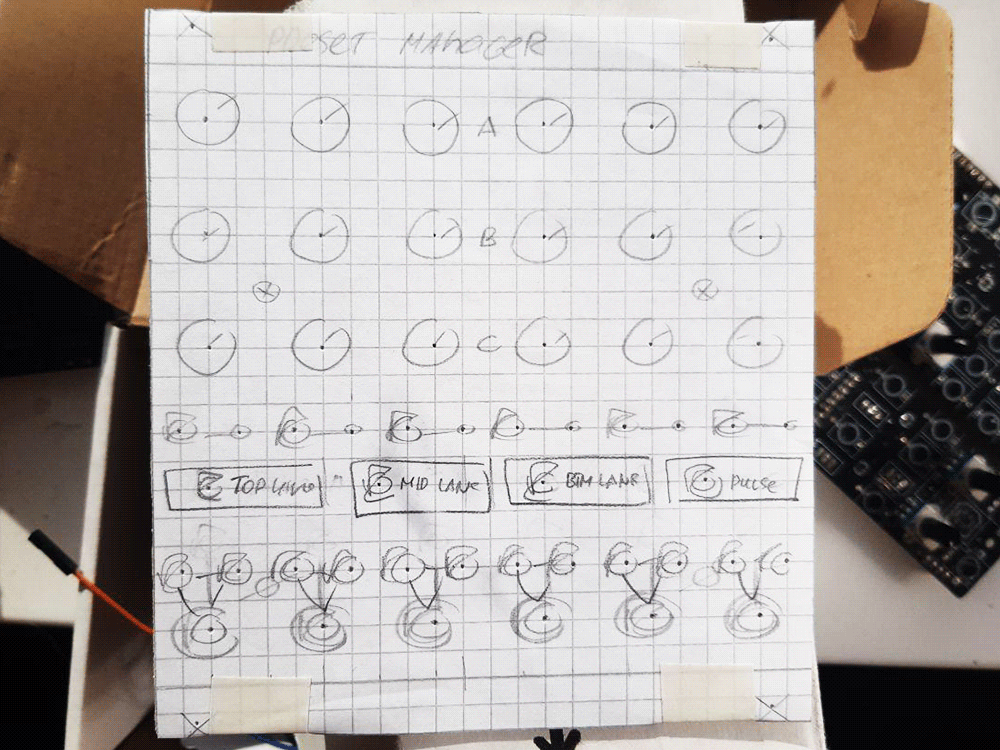
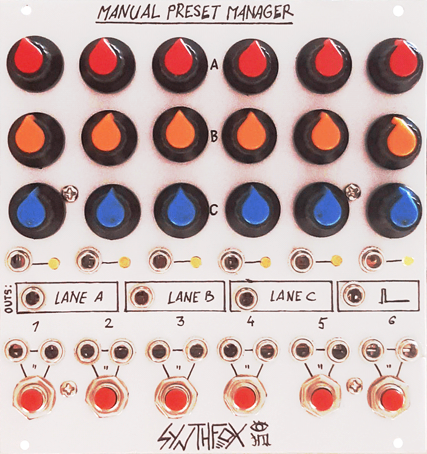
In all seriousness, the functionality of this device may seem outdated at first, and, for the most part, it is. This device is inspired by early preset managers and sequencing controllers by Serge and Buchla, but the circuit design itself has been made much simpler, cheaper and easier to understand - and there is room for more advanced features in the future. For now, however, this is a fun little controller. Push a button to select a column. An LED lights up above the button, meaning the column is now selected. Push another - and the new column gets selected, while the previous ones gets unselected. The voltages set with the three knobs of the column now appear on the LANE A, B and C outputs respectively. The jack next to the LED outputs a gate when the column is selected, and is at 0v when not. Don't want to push the buttons yourself? The two jacks above each button are the column set gate inputs, OR-wired together. One can use external voltages to automatically select a column. A pulse output on the right outputs a short, sharp pulse each time a button is pushed or a set gate is received.
Yes, but why?
While this may seem boring at the first glance, this is, in fact, a very useful device, especially if performing live, which i strive to do. The three dials can be used as macro parameters, majorly affecting multiple parameters inside the patch; then each column would represent a new sound scene, dictated by the dials' position. One can easily jump between the scenes with a mere button push. Column gate outputs can be used to enable or disable certain events, or fire an envelope only when a specific scene gets selected. A more classic approach would be to program pitch for, say, the bass drone layer, to then easily jump to the next accompanying sound, while still having time to play another instrument on top of the accompanying layer. Finally, in a pinch, this can be used as a keyboard with three set of values per key. Bear in mind, though, that the pulse output is indeed a very short pulse, as depicted on the faceplate, not a gate that holds high as long as any button is pressed, which limits the use of manual preset manager as a conventional keyboard, which it isn't to begin with.
The upside of this design is, while providing major macrocontrolling and soundscaping power, it comes at a fraction of the price and effort, as the circuit is dead simple, even though it requires quite a bit of explanation for one to understand what exactly is going on. This is quite a suitable project for someone a bit SDIY-stronger than a plain beginner!
Schematic
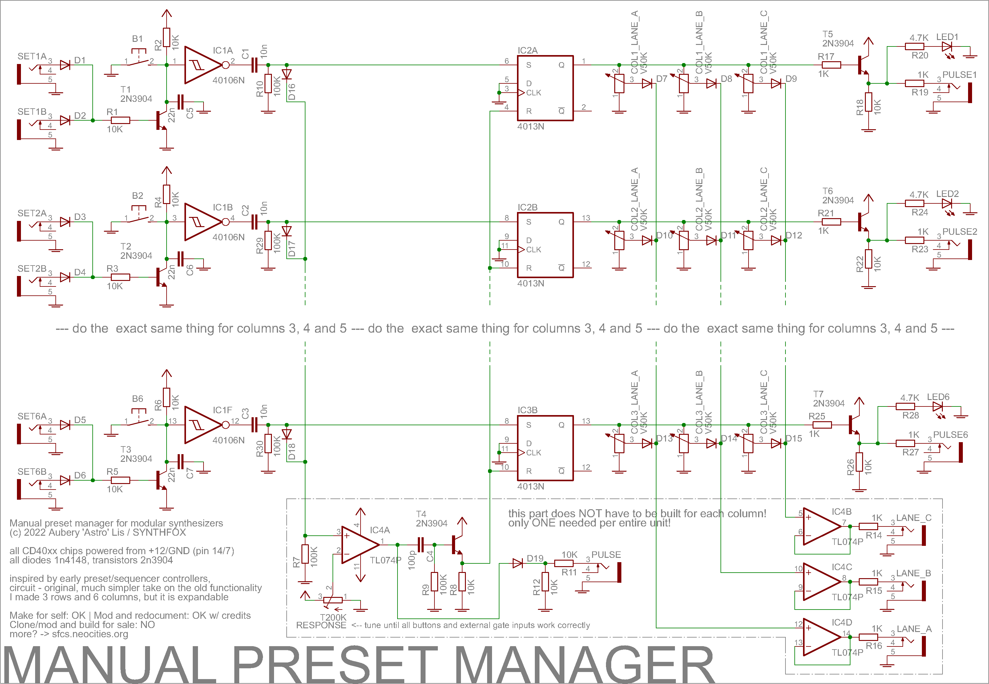
I highly recommend opening the schematic image in a separate tab to easily jump back and forth between it and the text. The circuit is dead simple, but there is a lot of text :D
The schematic is dead simple compared to other designs with similar functionality, and relies purely on exploiting the CD4013 logic chip, but first, a brief explanation of what is it at all. The CD4013 has two D-type flip-flops inside, which are kind of like single-bit memory cells. Each has a clock input and a data input; once the voltage on the clock pin flips to logic 1 (above ~7v from experience), whatever was on the data input pin - 0 or 1 - is written into the 'memory', quotation marks because it is just one bit, and it doesn't work like actual computer memory would. The value stored in the 'memory' is output at the Q out, with an inverted version available at the !Q output. This data-clock system takes priority over another system available on the 4013, the set and reset, inherited from S-R latches this design is based on. A logic high on the 'set' pin sets the 'memory bit' in the 4013 to 1, and likewise, a logic high on 'reset' resets the memory back to 0.
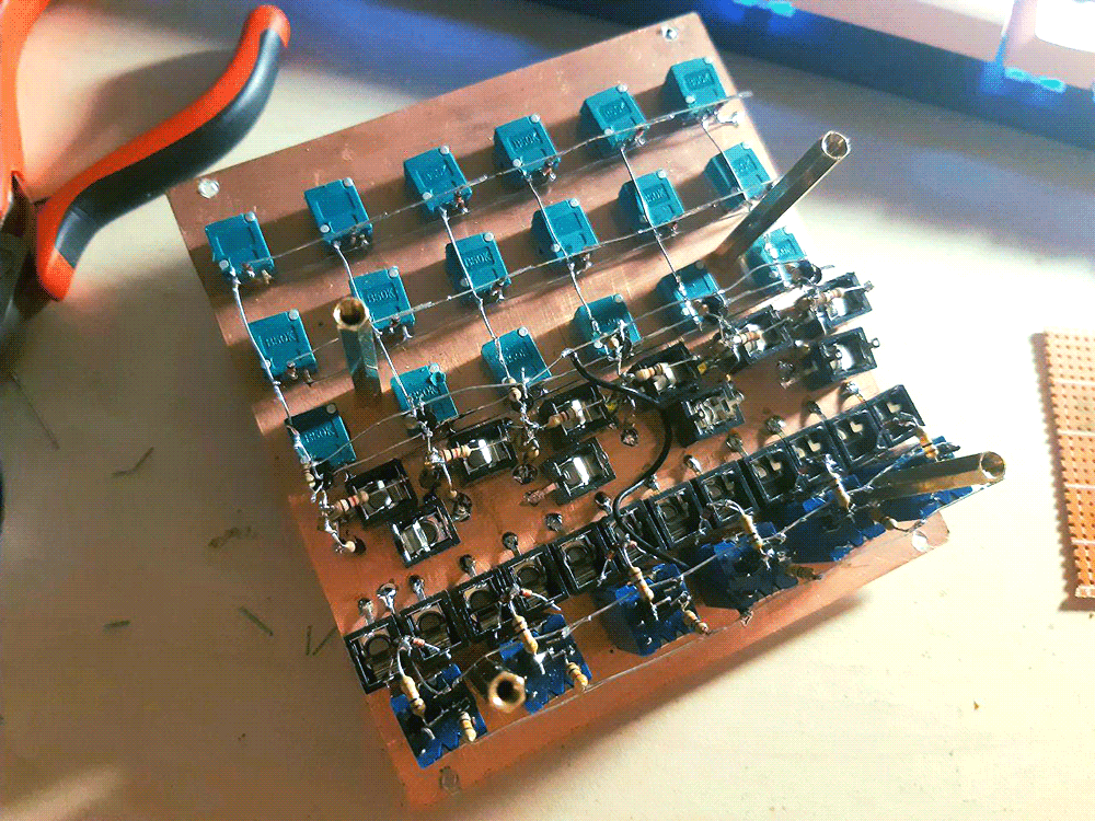
Keeping this all in mind, let's first look at the very left of the circuit. One of the reason i made 6 columns is because the CD40106 has exactly six hysteresis-enabled inverters on it. They are handy for debouncing buttons and produce clean rectangular pulses without any distorted short stray pulsing on state change. However, the 40106 has six inverters, and we want our default state of the output to be low (remember - the SR latch treats logic 1 as a cue to action), so for the topmost inverter, R2 pulls its input up to 12v, forcing its output to stay low by default. The button B1 shorts the inverter IC1A input to ground, which is an infinitely less resistive path than the 10K to +12v, so whenever you press the button, you drive the inverter output high. A capacitor C5 to ground does the debounce magick - improves the button stability, so to say. T1 below acts as another 'button', but externally controlled; a high enough voltage at its base will almost short the inverter input to ground, quite like the button, allowing for selection of columns with external signals. Finally, two jacks SET1A and SET1B are OR-wired using D1 and D2, and then go to the base of T1 through a 10k resistor. The inverter output is essentially passed through a highpass filter of C1/R10. This will transform the output of the inverter into a positive-going short spike when it flips to 1, and a negative-going one when it flips down: a very crude gate-to-trigger that just happens to work here. This is an important part, as it would be possible to select more than 1 column by pressing 2 buttons at once, if they weren't converted to these short spikes.
This design makes no use of the 4013 data/clock pins, so they are tied to ground. For the funny exploit, we only need the S-R latch functionality of the chip. The final desired result is for the core of the design to be an array of six logic gate outputs, only one of which is high at a time, and the rest are low. The gate that is high should be settable with an external pulse, which we already derived from the buttons using the inverters. This fits neatly into what 4013 has - the set and reset pins. The state of the chip when both set and reset pins are brought high is deemed 'invalid' in many datasheets, but the experimentally found truth is that the set pin takes priority at the Q output, while reset takes priority at the !Q output. This means, that if both set and reset pins are brought high, the Q output will stay high as long as the set pin is high, regardless of the reset pin during that. This means we can tie all the six latches' reset pins together and reset them on any of the spike pulses (any button pushed or any gate input pulsed), yet only set the correct selected latch, which will be the only one to stay set
Now the actual hacky part begins. This positive-going spike produced by the highpass RC filters after the inverters, that happens every time a button is pressed or an external gate is received, is good enough to use with the set input of the 4013. The negative spike gets reliably ignored by the latch and doesn't cause any issues. This takes care of setting the correct latch by pressing the respective button, or passing a high voltage to the gate in. But we still have to reset the rest of the latches, which would make sure we turn off the previously selected one. The outputs of the post-inverter high-pass filters are OR-wired together using diodes D16-D17-... and R7 , essentially formiing a signal that has all the positive pulses from all the buttons, with the negative ones removed. So, why not to use it to reset all the latches at once, since the selected one already gets reliably set by the highpassed spike output? Well, here's the trick - you have to 'let go' of the reset pin of the 4013 before you 'let go' of the set pin if you want Q to stay high afterwards. If the reset pin is high while set is already low, the latch will get reset to 0. And if a spike of exactly the same length is used at set and reset, it will bring both inputs high and low at exactly the same time, leading to unpredictable results. Sometimes it will latch correctly, most of the time Q will go high for a few microseconds, then go back to low, meaning that we just reset all the latches altogether and nothing is selected (bad).
The solution is to artificially shorten the result of ORring all the initial spikes, form an even shorter spike that will reset all the latches and go back to 0v way before the one spike that is currently setting the one correct latch ends. This is done with IC4A set up as a comparator. The RESPONSE trimm resistor is crucial, as it sets the length of the pulse that the comparator derives from all the spikes ORred. Tune it so that everything responds neatly. Too high and you will be able to select multiple columns (the reset will not go through), too low and the resetting spike will be too wide and will cause the selected latch to also be reset most times. The derived rectangular pulse is then passed through C4/R9, also a high-pass filter to spike it out, similarly to what happens after the inverters. However, while the resistor value for this highpass is the same as for the post-inverter ones, the capacitor is 100 times smaller, making the spike about the same times shorter. This, way shorter spike opens T4, which nearly shorts all the 4013 reset pins to +12v, pulled down to ground by R8 otherwise.
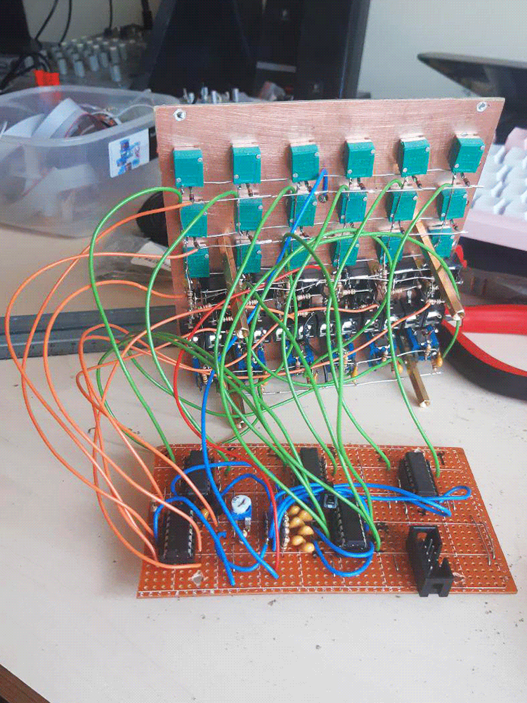
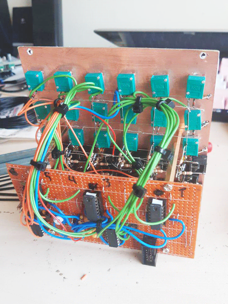
And there you have it! A very short pulse resets all the 4013 latches, while a somewhat longer pulse goes directly from the inverter only to one latch. Since the set input takes priority at the Q output of the 4013, there will be no glitching or delay associated with setting at resetting the latch at the same time, and we already have the hacky timing scheme sorted out to keep it high after all the pulses end. This is the only weird and hacky part of the circuit, the rest of the stuff to the right of the 4013s is the Usual. A bunch of potentiometers that divide the 4013 output, that are, again, OR-wired (stock up on diodes for this build) in a matrix-like fashion and buffered with IC4B/C/D, producing lane A/B/C outputs. Such setup is very common for the people's favourite, a CD4017-based sequencer. The only difference here is that I made 3 layers of pots instead of just 1, and have funky 4013-based selector instead of the 4017-based gate step sequencer before the potentiomters. The gate outputs are buffered with simple BJT logic buffers; i found out after using my own 4017-based step sequencer that using individual gate outs without buffering sometimes may detune the knob settings for that step/column by drawing significant current out of the chip, thus ruining the melody, if you have one going on. You can omit the buffers and wire the LED/jack resistors directly to the 4013 output if you don't care about the possible detuning. Finally, the output of the comparator, which is used to derive a shorter spike from the OR of all the long spikes, is passed through D19/R12 to shape it into 0..12v instead of -12..12v logic signal that IC4A actually outputs in this setup - this can be used to sync some external events, such as a sample-and-hold or a sequencer step, to the pressing of the buttons (or the receiving of the gates, for that matter). The pulse is naturally very narrow - not a button gate output - so, it does not make this into a convenient keyboard, except if you don't mind the lack of sustain and use fnuction generators with a trigger input that go up and back down regardless of the trigger length.
Some more circuit notes! If you wire the gate output of one column to the set input jack of the other, and vice versa, they will not oscillate between each other, but instead will latch up and be lit at the same time. Works for any number of rows connected, not useful at all. It is also possible to select 2 columns at the same time by routing the same exact pulse to both columns' set input jacks. This is pretty useless, too, but may be a side effect of using something like shift register-derived gates to drive the unit, as they may situatinally sync up perfectly. Finally, here's a mention of that you can have as many rows and columns as you wish: 6 columns in my case is dictated by the CD40106 being a hex ivnerter, and 3 rows just fit nicely into the faceplate space.
Media
A simple patch when cross-modulating VC-LFOs' speeds are also controlled by the MPM, as is one LFO's pulsewidth. Selecting a column changes the pattern the complex modulator provides for a VCO and a VCA processing its triangle out.
A more complicated patch with everything modulating everything and the MPM lanes acting kinda like macro controls, routed to a lot of destinations at once.
Pictures