About
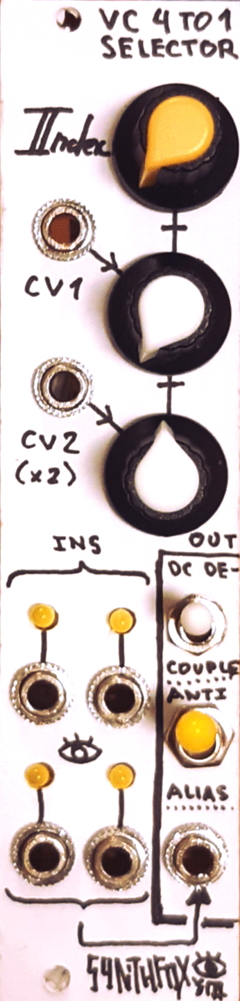
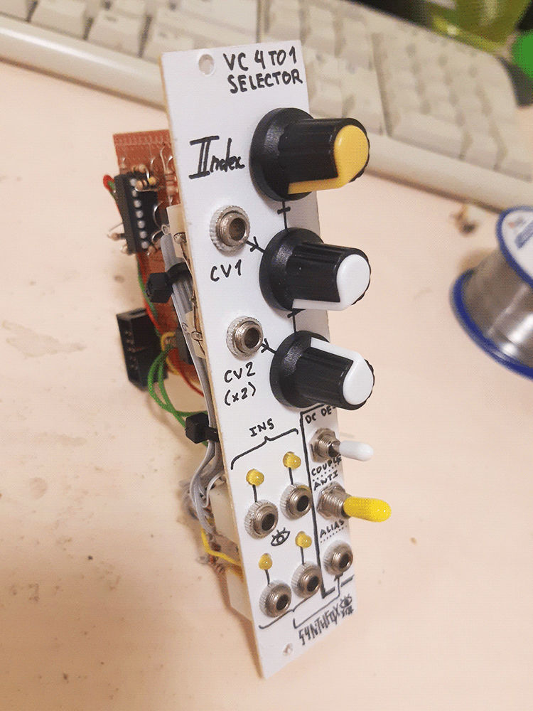
VC 4 To 1 Selector is another useful and universal utility module. Based on the Signal Switch by Rene Schmitz, it is a device that selects one of the four input signals and reproduces it on its single output jack. It covers the entire modular signal voltage range and has super low distortion, making it suitable for both CV and audio usage - and, naturally, binary logic signals, too.
Unlike many switches ruled by binary decoding (3 gate inputs ruling an 8 to 1 switch by representing a 3-bit number) or sequentially (a switch that cycles through 4 signals on a clock pulse), this one is voltage-controlled, making it less of a sequencing tool, but more of a universal switching device: the Index knob has four equally sized 'zones', in each of which one of the 4 inputs is selected. Two control voltage inputs with associated attenuators are added to the Index knob and can move the selection externally. The second CV in has a gain of 2 when its attenuator is fully clockwise, making the module suitable for being controlled by signals with relatively small peak to peak amplitude.
Additionally, the output has some switches to better fit into desired application. The DC Decoupling switch enables the dc-decoupling of the signal, also sometimes (mistakenly) called ac coupling. This means that the output will attempt to keep the signal centered around 0 volts as much as it can - makes it sound better for audio, generally useless for anything else. There also is an Antialias three-position switch: it enables slight lowpass filtering of the output, 'linking' the mismatched sharp edges of the switched signals with tiny glides. In center position, the filtering is disabled - all the sharp edges will be preserved, good for gritty, robotic sounds, or for sharp CVs. Up and Down positions enable slight and audable filtering, helping to remove unwanted pops from CVs or smooth out the audio.
This design has a glitch that's noticeable at audio-rate switching: between going between inputs B and C, the circuit lags a bit and selects A for a fraction of a moment. Pretty sure this is fixable by simply using dedicated comparator ICs instead of using an op-amp as a comparator. The antialiaser helps a lot against this glitch.
Schematic
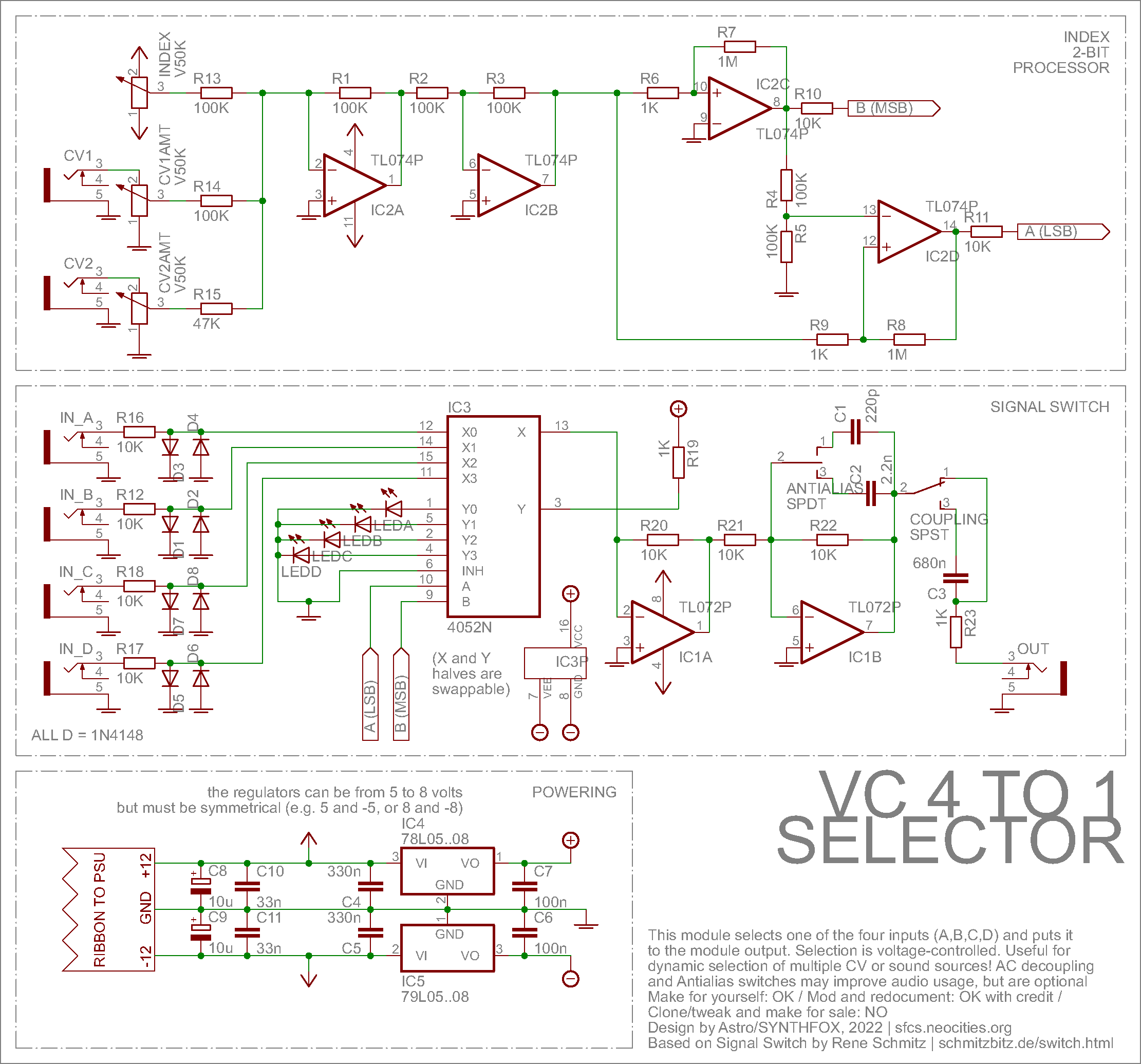
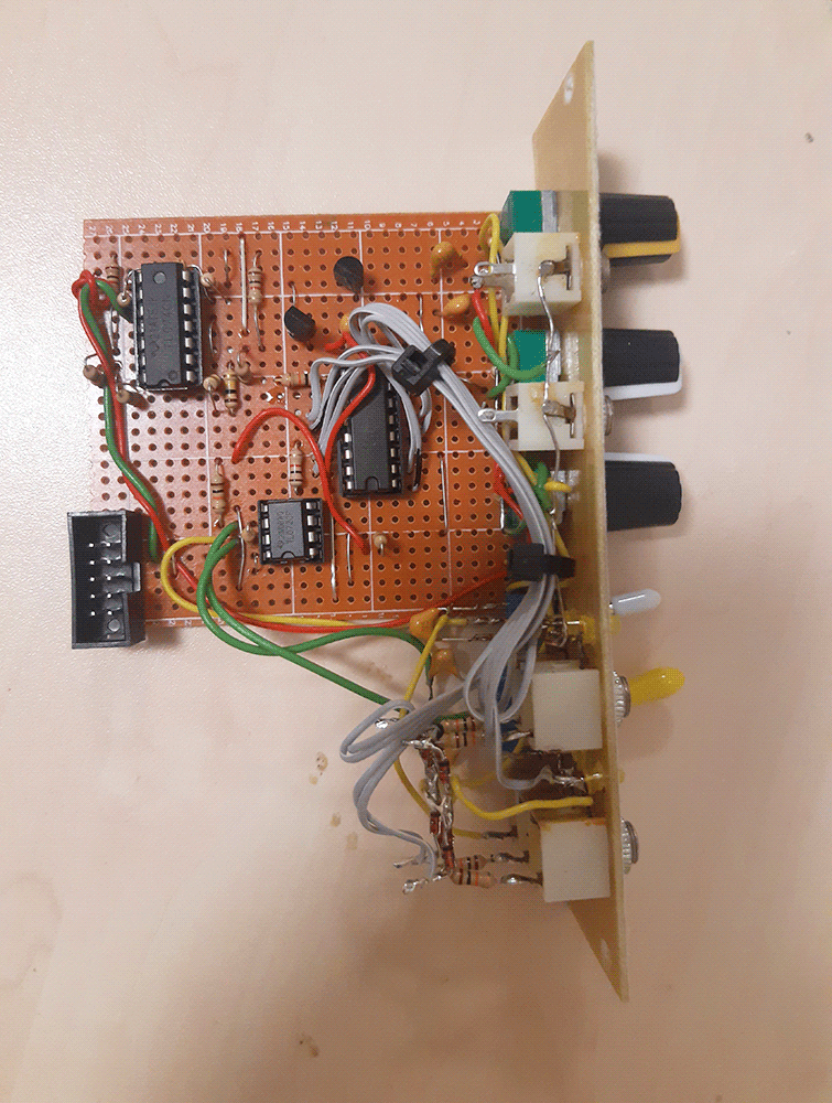
The schematic is broken down into three parts: the 2-bit ADC on top, the selector in the middle, and the powering in the bottom. I will break it down bottom to top, starting with the powering.
Unlike usual synth modules, this one has its own additional regulated power for the selector chip, CD4052. The chip features separate terminals for ground and negative voltage, allowing for a seamless bipolar operation - but also, the maximum difference between positive and negative voltage can be 18 volts, meaning it cannot be powered from +/-12v, as it will cause a 24v difference and the chip will pop and burn. For this reason, two small voltage regulator ICs are used, 78L08 and 79L08. The first one is a positive regulator that makes stable 8v out of 12v, the other one is a negative regulator that makes -8v out of -12v. The resulting difference is the safe 16 volts - it's OK to power the CD4052 from these regulated voltage sources. In fact, the regulators could as well be selected for +/-5v (78L05 and 79L05), or probably even +/-3v, but i deliberately chose the widest possible range, as to reduce the useless heat from dropping the voltage on ICs.
Now, take a look at the middle section. Its main character is the CD4052 - a CMOS chip that has two 4-1 multiplexers ("4 position switches"). gotta love how many nice dedicated CMOS chips there are! The CD4052 has two halves. Each shorts one of its numbered terminals (x0,x1,x2,x3 or y0,y1,y2,y3) to its common terminal (x or y) depending on what's going on at the A and B logic inputs. Both halves read the same A and B, so if x1 is selected, y1 is also selected. A and B inputs represent one of the four possible 2-bit binary numbers (00, 01, 10, 11): they treat a high voltage like a 1 and low voltage like a 0. What exactly are the thresholds of 'high' and 'low' is unknown to me, but i am driving these with +12 for high and -12 for low, through a 10K resistor so the internal CD40XX-style diode clamper does the job for me, probably in exchange for some wasted current. It works!
Ok, it selects - but it's powered from +/-8 volts - won't the signal get distorted? Well, here's where the genius of Rene Schmitz comes in. To have no voltage distortion, you should simply barely have any voltage difference at all across the switch; it's easier than it sounds. Note how each input (A,B,C,D) has a 10K resistor after it (don't mind the diodes for now). The IC1A/B after the switch form two unity-gain (gain=1) inverting op-amps in series, so basically a usual double-inversion voltage buffer. But the input of IC1A is connected directly to the CD4052, without a 10K resistor between them - that's because we want to exploit the virtual ground properties of the unity-gain inverting op-amp configuration to make the voltage difference across the switch as small as possible.
If we treat the switch like a short circuit between the selected input and IC1A for a moment, we can see how the 10K resistor after the input jack goes straight to the inverting input of IC1A, and the circuit forms a usual double-inverting unity-gain voltage buffer/summator,but with just 1 input in this case. IC1A will try to push as much voltage through R20 as is needed to make the resulting voltage at its - input equal to what's on the + input, which is grounded. This brings the whole 'line' between the resistor on the active input and IC1A - input to 0v: this is what's called a 'virtual ground', as it's not grounded per se, but the rest of the circuit will treat it as if it were.
In reality, CD4052 is not really a short circuit IC, so there will be a tiny voltage difference across it - yet so insignificant, that it barely adds any distortion. The two diodes on each input limit the input voltage to +/-0.7v to prevent overvoltage when switching, etc, so the voltage difference across the switch won't EVER exceed that. That's why it can be ran even off regulated +/-3 volts. The other half of the CD4052 is used in the opposite direction from the signal switching one - the common pin has +8v attached to it through 1K, and all outputs have LEDs to ground. The switch forms a +8v - 1K - LED - GND loop with one of the LEDs, depending on the selection. The LEDs are used to indicate which signal is currently selected. Look at the module closeup in the beginning of the page - the diodes above input jacks are these four diodes. Make sure the input connected to x0 gets the LED connected to y0, and so on..
Cool, now the only remaining thing to do is to drive the CD4052 logic inputs A and B so that we can scroll through the inputs with a knob. This means, there has to be an analog-to-digital converter (ADC) that takes in a voltage between -12..12v and represents it as two binary logic signals, representing one of the four 2-bit numbers. I threw together such a device on a single TL074 - somehow, i've never seen a circuit like this in the internet before, and i searched! Good job Aubery. This circuit works, but has a slight glitch mentioned above: this is the price you pay for using op-amps as comparators, instead of getting actual comparator ICs. Pretty sure it would fix itself with a dedicated dual comparator IC. Anyways, IC2A/B is your usual 2 op-amp double-inversion summator, quite like the one used for the switch hack, but an actual summator this time. IC2A outputs an inverted copy of the sum of the Index knob, CV1 and CV2. Note how R15 that sums up CV2 to the other signals is 47K instead of 100K: this makes its gain in particular 2 instead of unity-gain (1), allowing this particular input to amplify CVs. I made it so that smaller waves - say, 10v peak to peak - could be amplified to 20v peak to peak, to cover almost the entire possible voltage range. Not enough? Change R15 to 22K for a ~4 gain.
IC4B inverts the inverted sum to get the uninverted sum, and then this gets ADC'd by IC2C/D. This device is terribly simple: we divide the full voltage range (-12..+12v) into four zones: -12 to -6, -6 to 0, 0 to 6, 6 to 12. Then, we have to tell, which zone the input voltage fell into. First 'question' we answer is - is it above or below zero? This is 'answered' by IC2C - set up as a comparator, comparing the input to ground. It outputs +12V if the input is above 0v and -12 otherwise. R6/R7 form a hysteresis network for bounceless, noiseproof operation - read up on comparator hysteresis if confused. IC2C will drive the B input of the CD4052 - the upper, most significant bit. Since the numbers in binary go 00, 01, 10, 11 - it fits perfectly by being low in first two zones and high in the other two. Hooray, 1-bit ADC! Now, we have to see if the input is above 6v (if it's in the upper half) or above -6v (if it's in the lower half) to make it 2-bit. For that, the output of IC2C is divided by 2 with R4/R5 and fed to the inverting input of IC2D. It also is a comparator: in case IC2C is high (input is above 0), the voltage at its - terminal will be 6v, and IC2D will go low if the input is in the 0..6 zone, and high if it is in the 6..12 zone. However, if the input is negative, IC2C will go low, and IC2D will instead compare the ADC input to -6 volts, differenciating between the -12..-6 and the -6..0 zone. IC2D output is used to drive the A (lower, least significant bit) of the CD4052, as it goes low-high-low-high over the voltage span.
Just in case someone didn't get any of the very nicely written, extremely comprehencible explanation above, here's a table, too:
| Index+CV sum is in | IC1C output | V at IC1D inv. in | IC1D output | Encoded number | Decimal |
|---|---|---|---|---|---|
| -12..-6v | -12v (0) | -6v | -12v (0) | 00 | 0 |
| -6..0v | -12v (0) | -6v | 12v (1) | 01 | 1 |
| 0..6v | 12v (1) | 6v | -12v (0) | 10 | 2 |
| 6..12v | 12v (1) | 6v | 12v (1) | 11 | 3 |
Either this makes no sense, or by now you feel bored at my overexplanations of a simple 2-bit ADC, but the table is cool anyways. This turned out to be one useful subcircuit, and i believe it can be used in other projects. Maybe it could be further laddered down to 3 bit resolution in a similar fashion. It is inspired by the selector channel of the SFP24 Step Phrase Programmer - which works similarly, but is bulky and nowhere as neat, + only detects three states. This whole selector design takes very few parts and does quite a rad job, if you ask me, so go build it now!
Media
The VCO is modulated by one of the four sources (a CV sequence and three different oscillations) and then treated with the shaping gate and the delay
Audio rate switching of audio rate signal, both from the 40106 Dual VCO. AC coupling and antialias options come in handy.
A slightly more complicated patch - this module's role in it is switching between three types of filter response (BP, LP, HP) or silence as part of the delay's feedback loop.
Pictures