About
This is a monster of a module using a puny number of parts. One day I thought that the Serge Voltage Controlled Slope (sold by Elby, Bananalogue, and serving as a basis for many modern modules like Befaco Rampage etc) is way too complicated and half the parts can be thrown away. Also half of the resistors can be 100K, cause that's the ones i have a lot of. Surprisingly, i was correct!
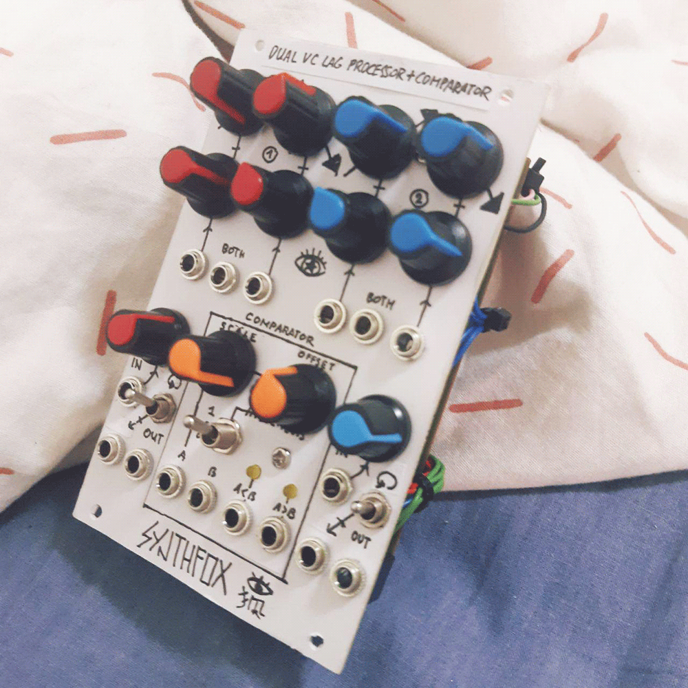
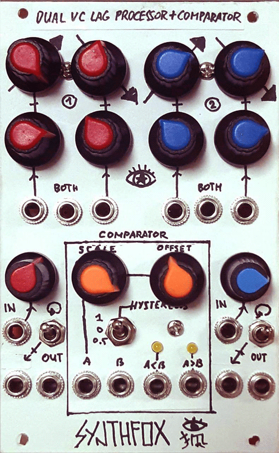
This module has two identical voltage-controlled lag processors (or slew limiters - it's just i already have a "vc slew" module) that build up on the barebones VCS core. Each features a rise time control and rise time cv input with an attenuator, same for the fall time, and a 'both' control that tracks exponentially (but will change response on changing the rise/fall time, so no 1v/o for you).
There is a signal input with an attenuator. There's no gate or trigger input, like on most VCS/USG derivatives, as this is not a clone, but a regrown core aimed for signal processing. Optionally, a cycle comparator/switch can be installed (that's what i did) - then the lag processor can become an LFO. The cycle comparator output is merely mixed down with the input jack, so cycling this lag processor and still feeding it signals brings up interesting patterns.
Additionally to the two lag processors, there's a comparator section inbetween them. It is also optional for your build, but i highly recommend it for it's an extremely versatile tool. Input A has offset and scale (attenuation) controls, whereas input B is passed to the comparator as is. The section has two gate outputs - one fires if voltage A (divided by scale pot and offset by the offset pot) is less than B, and the other is the inverse event. Lag processor 1 and 2 outputs are normalled to inputs A and B of the comparator respectively, which makes it compare the two lag processors' outs if nothing is patched in.
The comparator has another trick - the hysteresis switch. This makes input A have to "go an extra mile" before crossing B voltage up or down, which makes it have a sort of a 'window' - not to be confused with Serge envelope window out. This is very useful for cycling slew limiters not cyclable by default, comparing with more precision (no threshold border bouncing etc) and much more. Read more on hysteresis comparators if you're confused - it's a bit hard, but very useful!
TL:DR low part count, two VC slews with cycle, a cool comparator. Build it.
UPD 31 Oct 2021: after washing the board with flux "just in case", both lags started drifting downwards on rise setting lower than noon. After 5 hours of investigation and 2 additional prototypes for error reproduction, i found NOTHING, but both prototypes build by the old schematic were also drifting. Maybe the flux was somehow lowering the 4.7K base to ground resistor to about 2.7, or something. I changed up some resistor and capacitor values and now it works.
Schematic
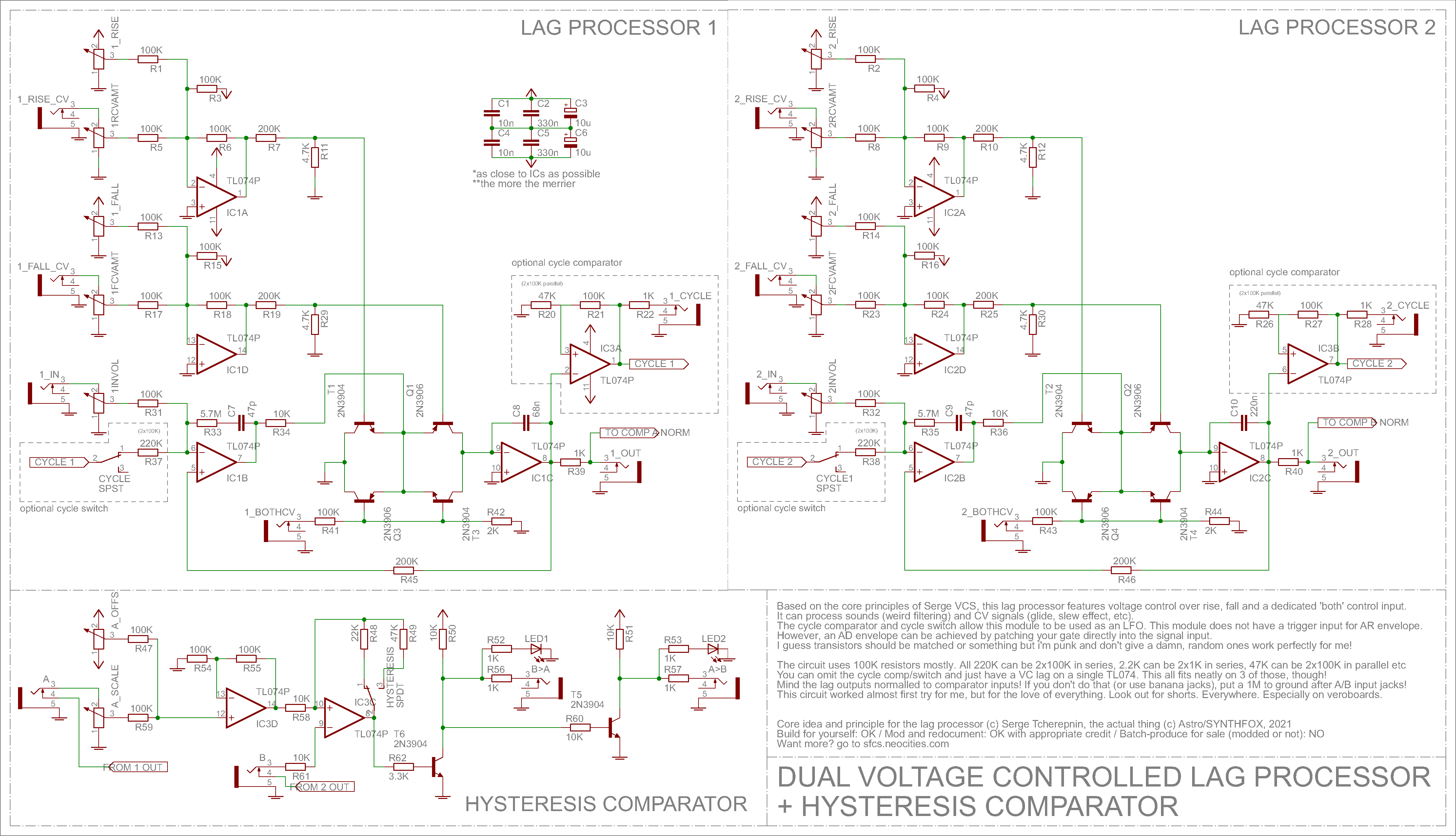
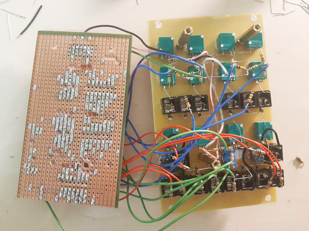
I took the VCS core (comparator/amplifier - transistor magick - integrator) and made the rest of the circuit use as few parts as possible. Also, as many resistors as possible were made 100K. If you want an in-depth analysis of the Serge VCS - go here, there's zero sense for me to retype all that goodness. Put simply: two op-amps on top each invert-sum a time control knob, a cv input with an attnuator, and -12 to offset the inverted sum to +12. They make the rise and fall control voltage sums. The output of these op-amps, ideally [+12v...0v], drive the cool transistor setup, about which you should read through that link really, but it sort of defines how fast the current from another op-amp feeding the transistor network (the comparator-amplifier one) charges and discharges the integrator that's after it. The output of the integrator is processed through a special comparator that allows cycling, and it goes back through a cycle switch to the input stage, which is a wicked comparator/amplifier feeding the transistor magick. No guarantees - this is how i see it, and i'm not a pro. Go read a good article.
I threw out all the triggering logic - i just wanted the slew limiting part. The rise/fall control input amplifiers were also simplified without making any difference to the action - except now rise and fall controls decrease the lag time as you turn them CW, just like on the rest of sane people's modules (the original has it vice versa). Some people argue that the transistors for the core should be matched, or something, but i picked some random 3904/3906s and it works perfectly.
The cycle part is something that I made from scratch - it's, again, a funky usage of a hysteresis comparator. In my previous module, the Dual VCLFO, i used this trick to make the LFO do the LFOscillation, so you can go check it and see how it works. Here it's the same thing, except the simple op-amp integrator has been replaced with the entire lag processor, and the comparator's inputs have been swapped in order to invert the comparison result (because the lag processor, unlike a simple op amp integrator, is non-inverting).
R33 for lag 1 and R35 for lag 2 were 10M in the original schematic: i tried various resistors from 1M to 10M and there was barely any difference, so i picked the ones i had the most of. The capacitor that is connected to it should be in picofarades, but i ran out of 47p's on the first lag, so the second one has 33p and has the same frequency range. The actual range is set by C8 (C10 for lag 2) and the more you increase it, the longer times you will get, but it also caps the top frequency when it cycles. 22n is optimal, although 330n works just as fine, and even goes to sound range still.
As for the hysteresis comparator in the middle of the faceplate - it's fairly simple and very useful: we attenuate input A, 1:1 passive-sum it with the offset knob and amplify it by 2 with IC3D to make up for the passive summator. Then this sum is compared to input B on IC3C, and there is a hysteresis loop around it. I used a switch for to switch between the two resistors the sake of simplicity. You can pick different values - what matters here is the proportion between R58 and whatever goes back to it from IC3C output. If it's lower than R58, you're gonna have troubles getting the comparator out of the hysteresis window, so i propose it be at least 1.5*R58. You may as well install a 10K resistor and a 50K pot in series around the op-amp instead for smooth control of the hysteresis window size. Big resistance (small hysteresis) can be useful for turning audable noise into gates that also make sense.
Finally, IC3C output feeds a simple BJT-based inverter chain. Since IC3C detects when A is more than B, the first inverter gives B>A (or A<B, as on my faceplae). Reinvert it with another BJT and you get an A>B gate out. The gates are a bit weaker than my usual ~12v gates (10K resistor to VCC, yadda yadda) but seems to be triggering most stuff no problem.
UPD 29 OCT 2021: i found the hysteresis effect with the original values way too big, so i decreased R58 from 10K to 3.3K - now the range is satisfactory for me. This change is already reflected in the shematic above. You could use a 10K trimpot out there and select what's good for you 'by ear'.
UPD 31 OCT 2021: After washing the board, both lags started drifting on low rise settings. I have no clue why and how, but basically R7, R10, R19 and R25 are now 200K instead of 100K (two 100K in series if you don't have any), and the integrator capacitors' values got bigger. 68n makes the range moderate LFO to moderate audio frequencies, 220 goes into slow LFO and low audio. Although this works now, i feel like the range could be improved. This is NOT a perfect design. Any cooperation is appreciated!
Media
Basic lag processing. Both lags process different 7-step sequences coming from the Step Phrase Programmer - one controls the VCO pitch, other controls the VCF cutoff. Lag time goes from seemingly instant to literally averaging the input over time.
Cycling one lag processor and using it as an LFO for a filter here. Note how because the cycle comparator works around 0v, the LFO turns out bipolar! Not something you get from cycling a VCS. To get a unipolar envelope, patch a unipolar gate to the lag input.
The hysteresis comparator section can be used separately with its A and B inputs. Here, i patched a sawtooth to input B, and left input A unpatched - so cycling lag 1 is going into it. Messing with scale and offset does different PWM effects at the outputs!
Put the A>B output to lag 2 both cv input, rise full CW for both lags, fall about 1 o'clock for lag 1 and about 2 o'clock for lag 2, play a bit with the comparator knobs and you get a bouncing ball! Presumably. At least i totally do.
The X-Y Controller is controlling the VCO pitch and some parameters of both lag processors. Both of them are cycled, the output of lag 1 is patched to rise and fall CV of lag 2, and the comparator A>B output goes to lag 1 fall (or something!). Lag 2 output is used to control both the pitch and the volume o the VCO. Self-patching this thing seems like a huge soruce of wicked voltages.
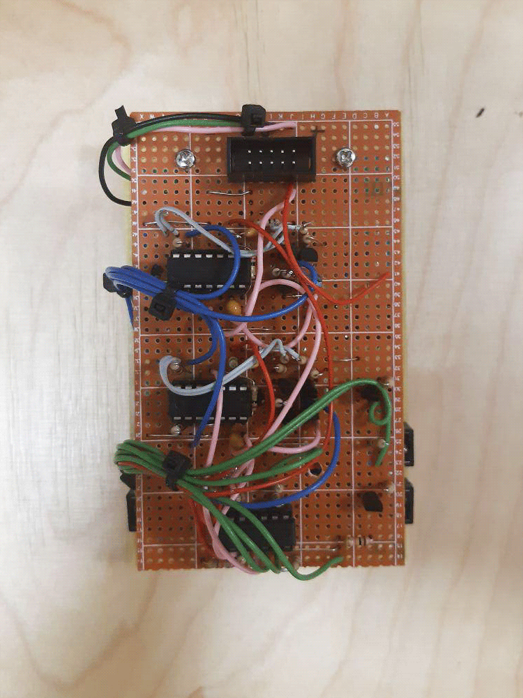
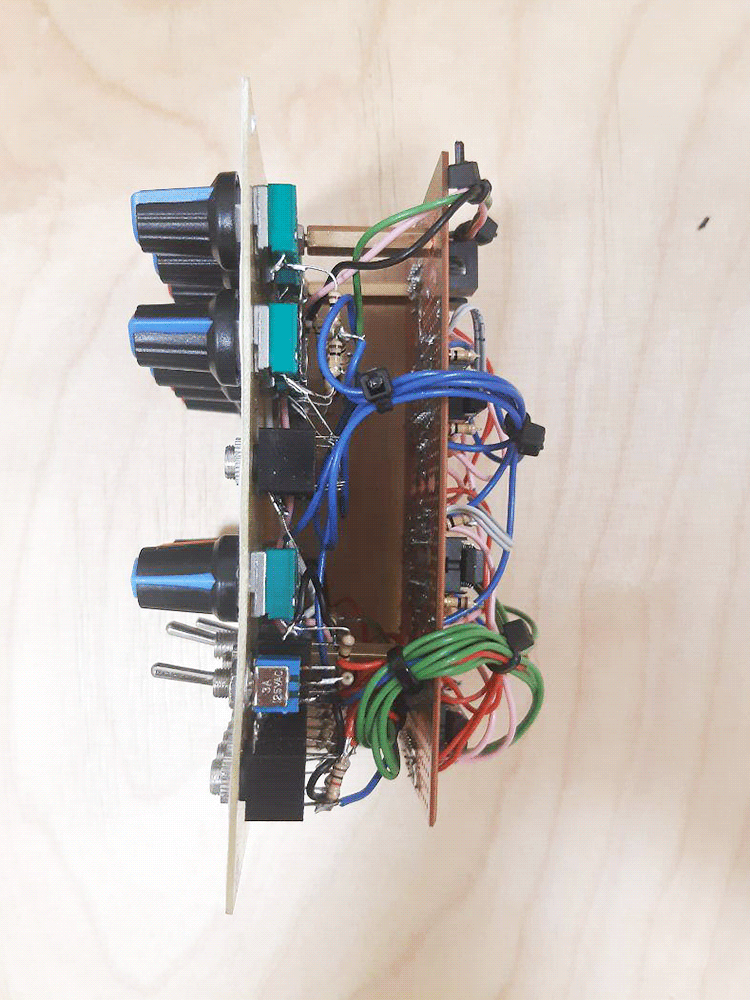
Pictures