About
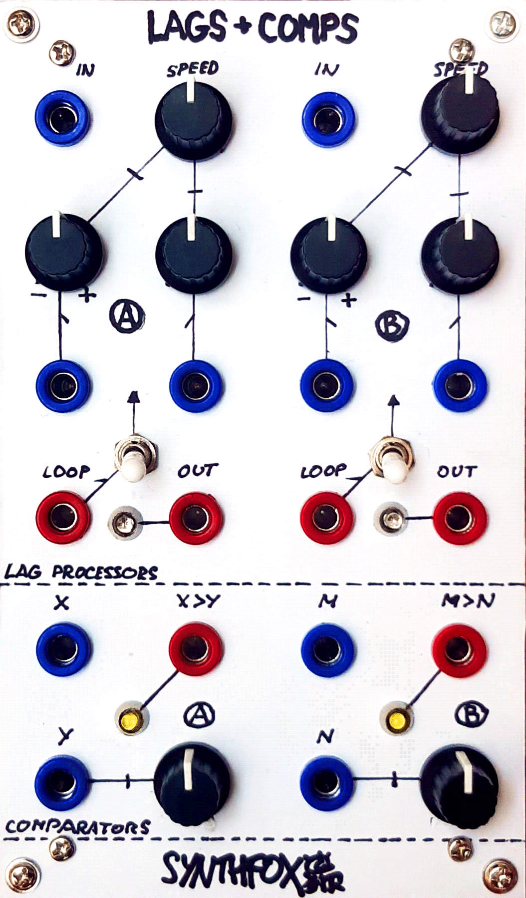
A module that's initially intednded to be a quick and easy modulation source and processor, but goes way beyound just that, the Lag Processors + Comparators design has two VC direction-insensitive lag processors and two small hysteresis comparators.
The lag processor's (or slew limiter's) job is to process an input signal so that the output is a smoothed out, 'inertial' version of the input signal. This is useful if you want to add glide to your CV sequence, shape a trapezoid out of a squarewave LFO, or even smoothly filter out audio. The secondary function of the lag is to be an oscillator: with a flick of a switch, the LOOP output gets summed up with the IN jack, and the module starts oscillating, as long as the input is in the range of about +-1.5 volts. Otherwise, the oscillation gets overridden by the input signal. When cycling, the lag processor produces a high-amplitude squarewave at the LOOP output and a 10Vpp triangle at the OUT output. Both lag processors have a SPEED control, which determine the lag/oscillation speed, and two CV inputs over it: one attenuated, one attenuverted. It's possible to drive the lag speed above the SPEED knob highest settings with an external CV, but not lower than the lowest setting.
Below the dual lag processor are the two comparators. The output indicates with a bipolar high-amplitude logic signal (+12 = 1, -12 = 0) if the voltage on the upper input jack is more (1) or less (0) than the sum of the voltages of the knob and the lower input jack. The comparator has a small, but existent hystersis, and won't jitter if the inputs are exactly the same. Not that useful on its own, this section really shines in complex patches as an 'event detector', or even in simpler application, such as a PWM pulse shaper for a triangle's sawtooth output, a gate amplifier/inverter, and so on. The knob works like a -12..+12v offset, but starts being a -3...3v offset if something is patched to the input jack Y (N).
Schematic
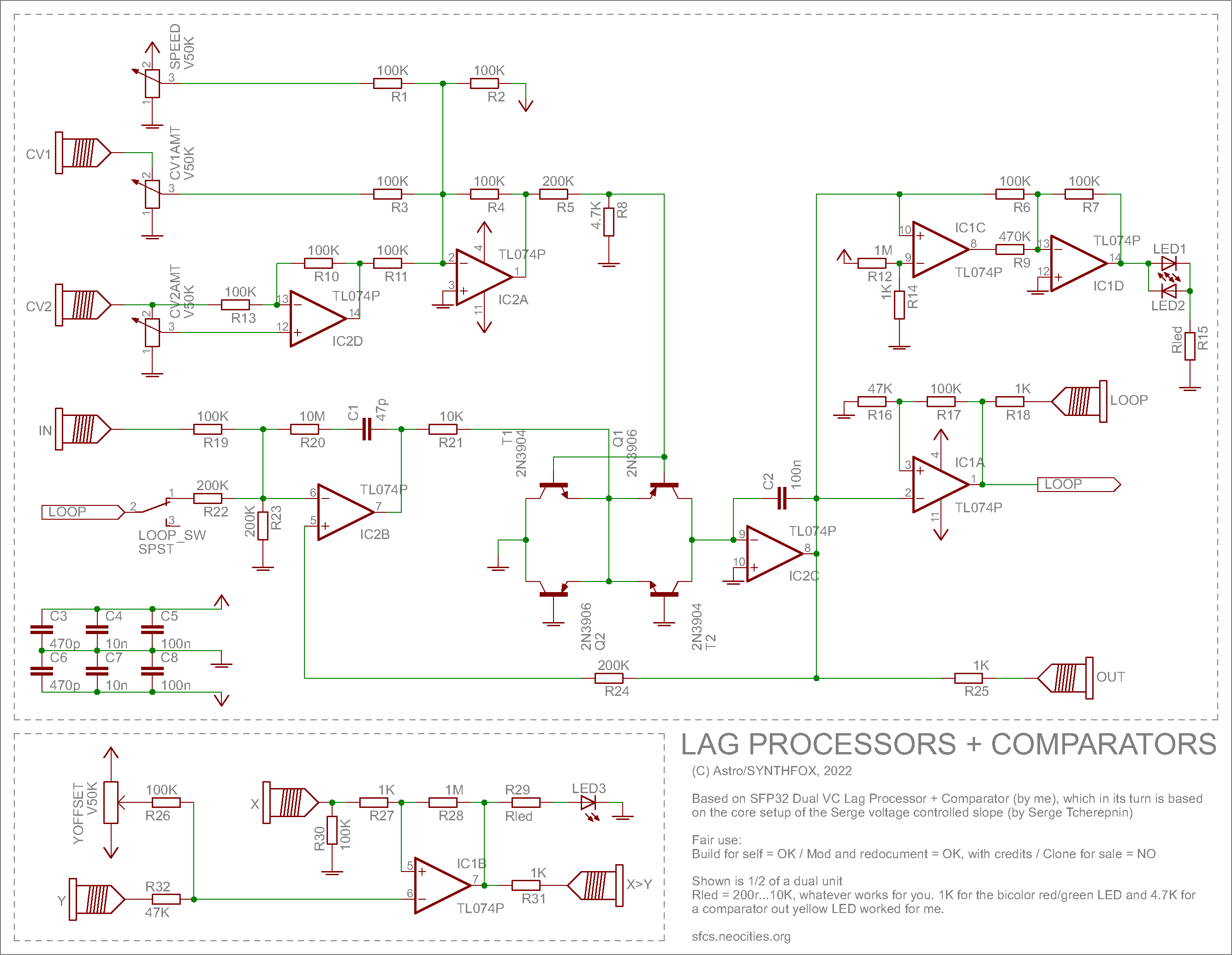
This lag processor part of the schematic is almost a full copy of the Dual VC Lag Processor + Comparator SFP series module. For an explanation on how this design works, please, visit the page; on this page are the descriptions of the changes introduced to the SFP design.
The rise and fall control have been merged into the single speed control, and the freed-up op-amp has been reused for CV2 attenuverter action, made by the kassutronics' simple design. The ALL cv input has been removed due to its redundancy, although the result is that in cycle mode, the shape is ever so slightly asymmetrical: maybe grounding T1/Q1 bases and using T2/Q2 bases as voltage tonrol tap would achieve better range and symmetry - this is to be tested for the final version of this design. The input attenuator has been removed, and R23 200K to ground replaces the pulldown effect the potentiometer had; without R23, the output of the processor may go wild at any time.
The output received a very buff LED indicator: IC1C compares the lag out to a tiny positive voltage to provide offset, and IC1D inverts-mixes this offset in a small proportion with a full-sized copy of the lag output, all to smoothly drive a bidirectional bicolor LED indicator. If you're too lazy to build this - at least buffer the output of the lag proc with one op-amp before the LED, as otherwise it will cause a significant voltage drop. Or don't use an LED at all, but hey, they are neat, especially in these metallic holders.
The comparator has been taken from the Control Combomodule shift core generator input section, as they showed themselves very robust and simple. R27/R28 add some hysteresis to the comparator, meaning it won't jitter at all when the X and Y+offset voltages are very similar The Y input and offset summing resistors R26/R32 are picked so that the offset knob is full-range +-12v when nothing is patched to Y, but becomes a rather subtle +-3V offset when there's something patched into it.
Media
A lag processor smoothing out the Control Combomodule random stepped voltage and modulating an Oscillator with the result
Same lag processor, same oscillator, but now the input is removed from the lag, and it is set to cycle. Testing the range of the speed knob.
A complex modulation source using crossmodulation of lag processors and comparison of them through the comparators, feeding the results back to the lag processors.
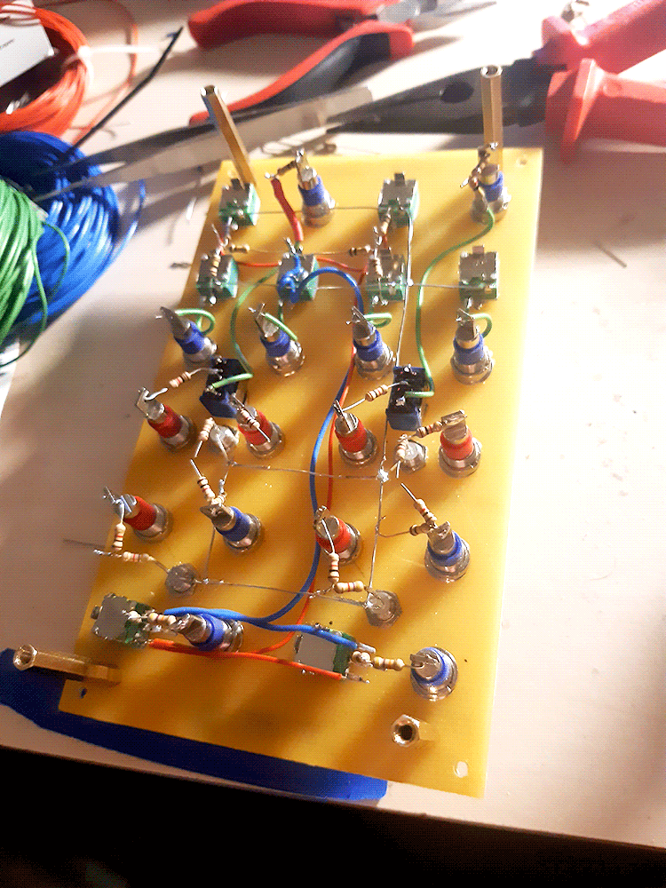
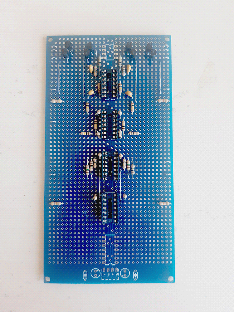
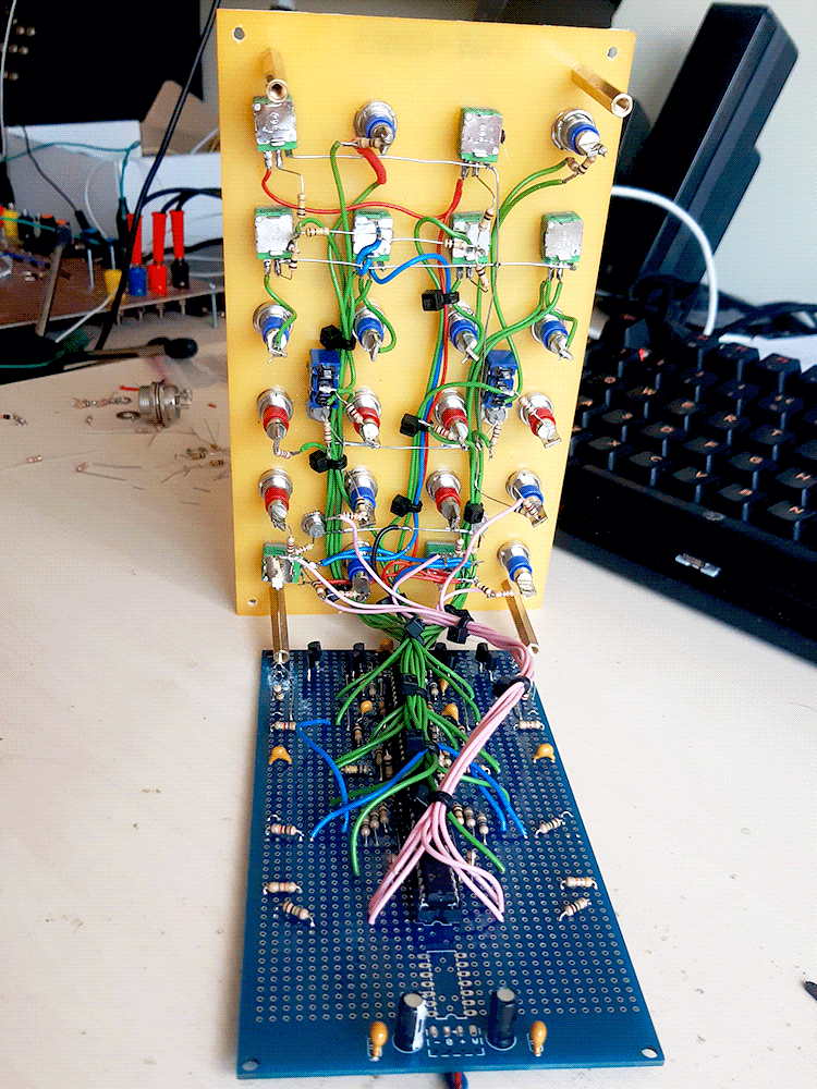
Pictures