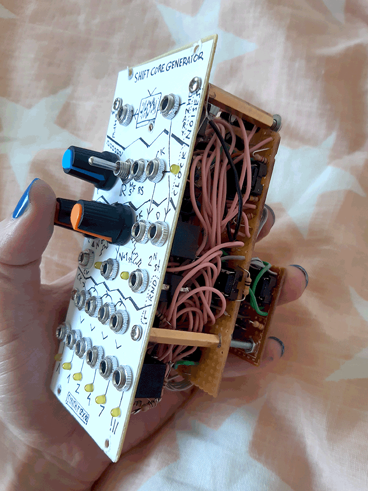
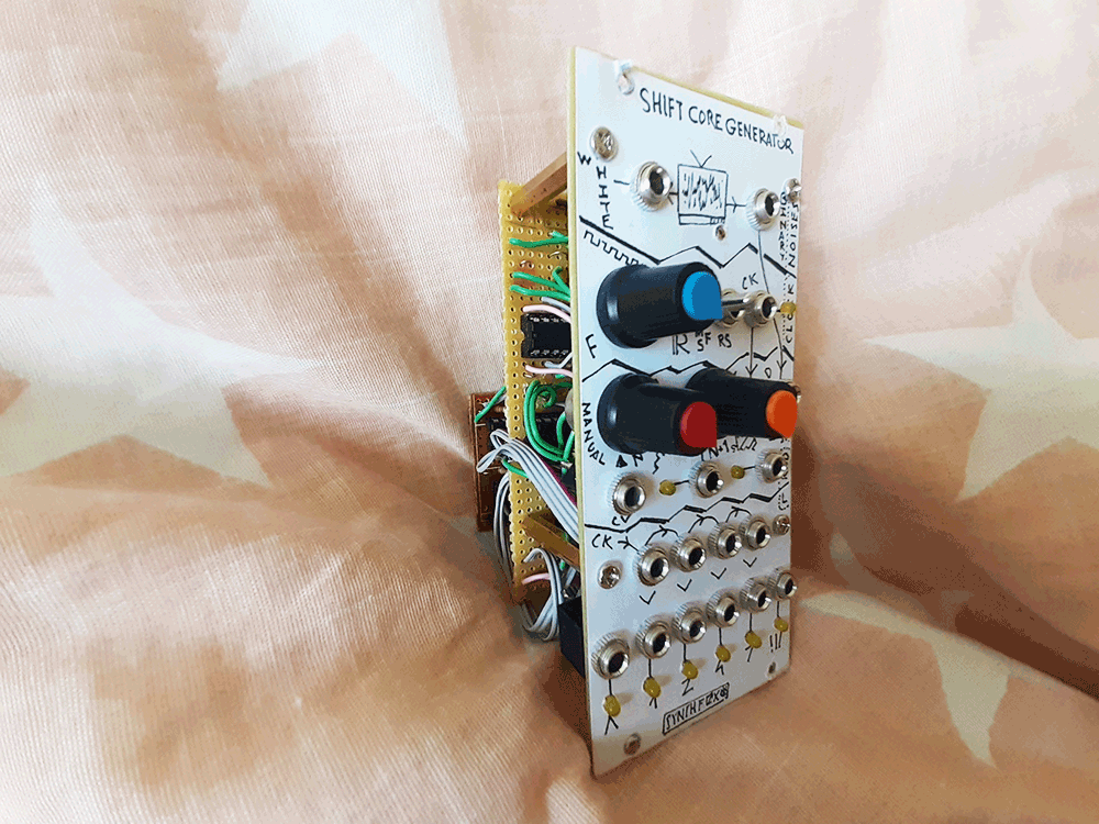
About
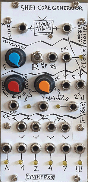
Shift Core Generator is a complex ready-to-rumble randomcentric CV and gate source. Inspired by Doepfer 149-1 and Buchla model 266, this module has a different generation algorithm on the inside and takes on its own route with what it does, but the main thing is still there: the stepped random volage outputs with control over how many states they can take.
UPD 12 APR 2022: This design served me for good 2+ years, but have now been replaced with a much better one. This one still works very well, but the new take on the same needs covers them way more efficiently, if you ask me, so maybe check the new one out.
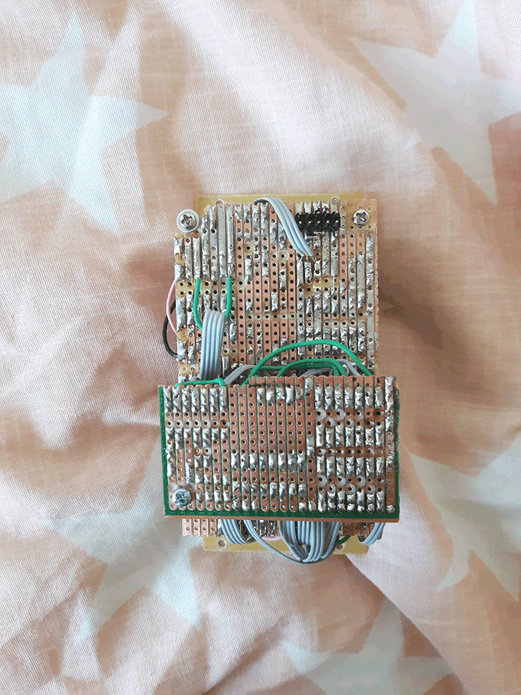
This module is relatively complex: if you decide to make it, prepare for a lot of debugging and messarounds. The build is not recommended for novice SDIYers.
The module is broken up into 4 blocks. The topmost one is the noise generator that outputs white noise and what i call "binary noise' or "binary garbage" - the version of white noise that was passed through a pre-set threshold comparator and output a fast, random stream shaped closer to gate signals than any kind of noise.
The second block below the noise section is a simple, non-CVable clock generator. It's a quick utility to get the thing started: it has a frequency control, a range switch to toggle between audio, clock and slow ambient clock modes, a hard-sync input (the clock will stop while there's a logic 1 on this input; a short spike will reset the clock) and the clock output.
Below the two is the "shift core": it takes in a data input, a clock input, and generates its internal state based on that and its previous state. Clock has the on-board clock normalized to it, and data also has the binary noise out of the noise block normalized to it. In this block are the 2 main results of the module: the N+1 states out and 2^N states output. These are stepped random voltages derived from the shift register core. N can be controlled manually and with an external voltage, and ranges from 1 to 8. The N+1 output thus can output from 2 to 9 values, evenly spaced voltage-wise: one can put this output to their 1 v/oct (or just exponentically VCable) VCO, and tune the CV amount to have the VCO stepping in semitones, thirds, or any other equal intervals. This output has a dedicated attenuator (the orange knob) to control the amount. The 2^N output can take from 2 to 256 (2^8) random stepped values which are NOT evenly spaced: you won't be able to get pure semitones, or other intervals, from it - so it is more suitable for control over filters, folders, and so on - that is, if you want melodic things to happen! Otherwise a pretty neat voltage output to control pretty much anything. This output has no attenuator.
With N increasing, the N+1 output will start reaching higher and higher values; on lower N values it will roll in the bottom. The N^2 output has a pretty huge span even with N=1, and increasing N will increase the 'resolution' of this output - it still will get some higher values, too, but also it will start having more and more steps between existing values with increasing N.
Finally, on the bottom is the Memory Gates block. It has four "binary sample-and-hold" circuits, which will sample a certain step of the shift register on a trigger signal. The steps available are 1, 2, 4 and 7. Reason for that is the number of steps between them increases between each pair (0, 1 and 2 steps between sampled steps respectively). By default, all trigger inputs for these memory gates are normalized to the internal clock, so by default it will just show the contents of the shift registers at given steps on each clock count. However, you can bring the module itself to audable frequencies, but trigger the memory gates with an external, tempo-setting clock: this way, you will get all sorts of randomesqe gate combinations without the "shifting" effect and dependency. To the left of the four gates is a XOR output: it outputs XOR of XORs the 4 memory gates' outs by pairs, so, kind of a "XOR Cascade" going on. The additional output to the right is a NOR of the inverted memory gate outs, which effectively is an AND of the uninverted ones as well. The outputs of the memory gates section can be used as drum triggers, envelope gates, or - with propper attenuation - as stepped 2-state CVs.
Schematic
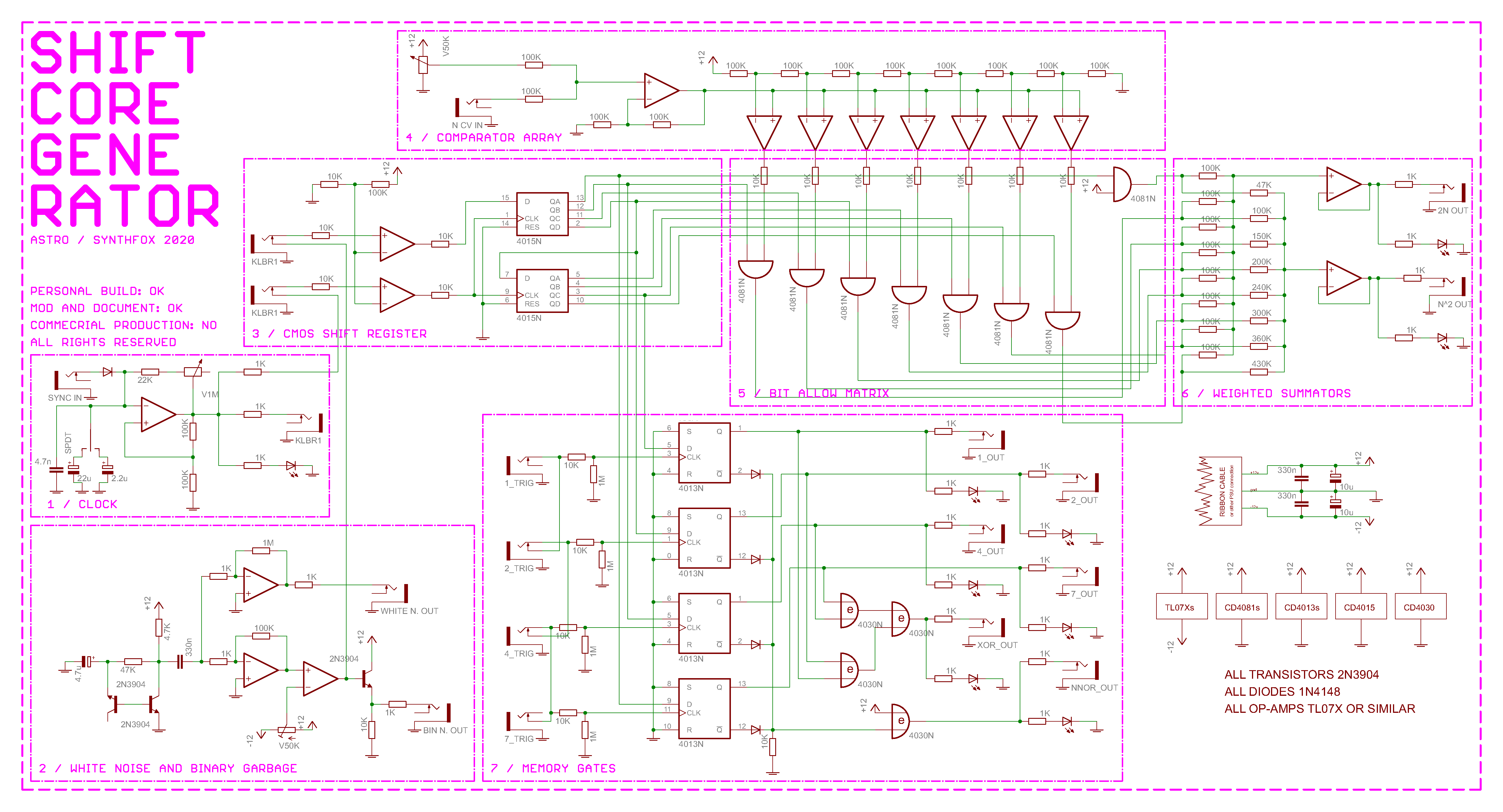
I decided to break up the schematic into numbered blocks for ease of explanation. It's not hard to understand, but quite complex on its own. The first block is the clock generator: a very simple op-amp squarewave generator. You can find explanations on its working principle - it works as pretty much any other relaxation oscillator would (for example, the CD40106 VCO). The only deviations from the classic circuit is that i replaced the feedback resistor with a 1M frequency control potentiometer in series with a 22K resistor to avoid zero resistance, added a switch that connects one of the bigger capacitors (or none, note that the swith is SPDT) in parallel to the audio-rate capacitor to give other frequency ranges, and a sync input, which will reset the clock on a short spike or stop it on a continuous logic 1.
Below the clock section is the noise generator. The core of this circuit is a reverse-breakdown transistor, the leftmost one. Then it gets buffered by another transistor, and amplified by 1000 for a white noise output, and by 100 and then processed with a comparator for binary noise. The trimm resistor that sets the threshold is very touchy and it's easier to tune it by ear when the circuit is complete: just find a point where the N+1 output doesn't incline too much towards the lower or higher values with N at the maximum.
Above the clock and the noise generator is block 3 - CMOS shift register. This is the shift core, that comes in a nifty DIL16 package. Pretty cool, right? The only thing we need to do with it is - process the data and clock inputs with comparators set to about 1/11(VCC) threshold so we can use sounds and other non-gate signals as clock or data inputs.
Above it is block 4 - comparator array. This is a subcircuit that sets our N: it's basically the comparators part of a flash ADC. First, we get a non-inverted sum of the manual N control and external N CV, and then pass it through an array of comparators, to their positive inputs. The negative inputs are chained in a huge volage divider snake, from +12V to ground, so we have 7 evenly spaced voltages on the negative inputs of the comparators. Note that none of the - inputs will get +12v or 0v, because the ground and +v are also connected through the same resistors. This is important, because if you imagine a sweep of the manual control handle - from 0 to maximum - at first, all the comparators output negative. Then as you cross the first threshold, the rightmost comparator will turn positive. Then the second, third, and so on, as the knob goes more and more towards +V. Finally, the last comparator turns positive BEFORE the handle is fully CW - there's still some space left.
The outputs of the comparator array are used to allow/unallow shift register's outputs to contrubute to the stepped voltage outputs in block 5 Bit Allow Matrix. First bit of the shiftreg is buffered through a 4081 AND with the other input tied to VCC. This bit will always be allowed. The other bits, starting from the second and finishing with the eigth, are ANDed with comparator outputs. The second bit is ANDed with the rightmost one: this way, once we turn the N control knob a little bit to cross the first comparator's threshold point, we will have bit 1 and 2 contributing to the random voltage outputs. When we turn the N control a bit more, the second comparator will light up, enabling the third bit of the shift register. This will happen until the seventh, leftmost comparator of the comparator array comes positive, enables the last, 8th bit of the shift register, and all eight bits are enabled.
The enabled bits then contribute to two different summators at block 6, Weighted Summators. One of them sums them up through same resistors, so every bit has the same "weigth" in the final sum. This is the N+1 output: because it doesn't matter WHICH bit is 1, but it only matters how many 1s and 0s we have in general, and we can have from 1 to 8 bits contributing to this sum, the lowest number we can get is 2 (one bit enabled, either 1 or 0) and the most states we can get is 9 (from 00000000, through 10000000, 11000000 ... 11111110 to 11111111). The other summator outputs an unequally weighted sum, and it is our 2^N states output. Each bit will contribute a different weight to the final sum, so it does matter, which ones exactly are on and off - so unlike with the equally weighted sum, for which if any 3 bits are on it will give the same sum, here it does matter which bits those were. This way, we have 8 digits, each can have 2 states, so we get 2^8=256 possible states. In my circuit, the first bit has the most weigth and the last bit has the least. This way, voltage jumps are possible. If the order was reversed, for example, the output would go around in more even and approximate steps. You can do both, or even do one with random order of random valued resistors, to get different combination possibilities!
Finally, there's the memory gate section down below - the last, 7th block. It is very simple: just 2 CD4013s used as one-bit "memory cells": set and reset tied to ground, the output of the shift register core which is getting 'sampled' goes to the data input, and the clock is just doing its job. The inverted outputs of the CD4013 are diode-OR'd and inverted with 1/4 of the 4030 XOR. Other three XOR gates are used to combine a XOR output of uninverted 4013 outputs. Fairly easy stuff!
Media
Demonstration of the N+1 output. Doepfer A-110 VCO is the sound source. CV amount is tuned by ear so that the VCO steps in fifths. I slowly turn the N control up and then back down. Note how higher and higher values start generating, and then disappear.
Same as above, bur for the 2^N output. It generates a way different random value stream!
A little demo patch, using both random stepped voltage outs of the module.
Same patch as above, but the N+1 and the 2^N outputs got swapped places. Feel the difference!
A recording of the module controlling a bunch of percussion sounds. The N+1 and 2^N outs are also used to control some of the sounds' parameters. No external clocks, gates, sequencers or whatsoever.
Doepfer A-110 VCO frequency-modulated by a slow triangle LFO used as a clock source. Data source is built-in binary garbage. Another, slightly faster LFO controls the N value. And we get voltage-controlled gameboyish noises! First is the N+1 noise, then the 2^N noise, then the gates XOR output noise, and finally the NOR output noise. Lots of different flavours of noise!
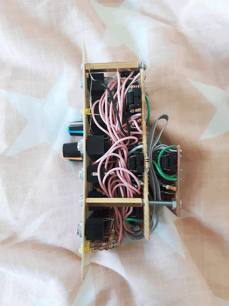
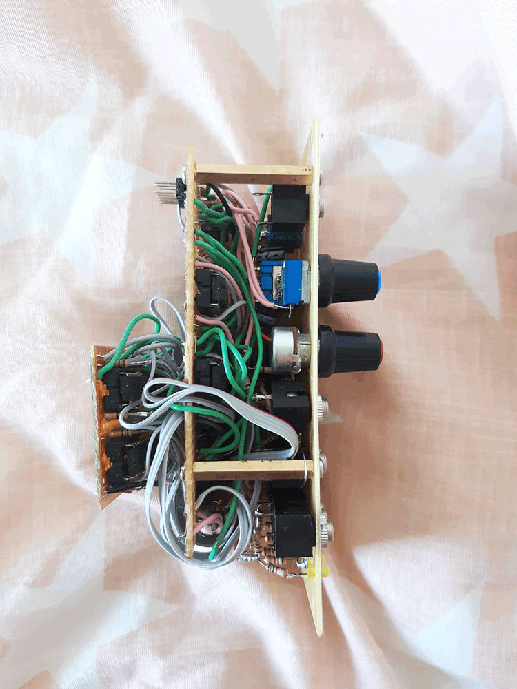
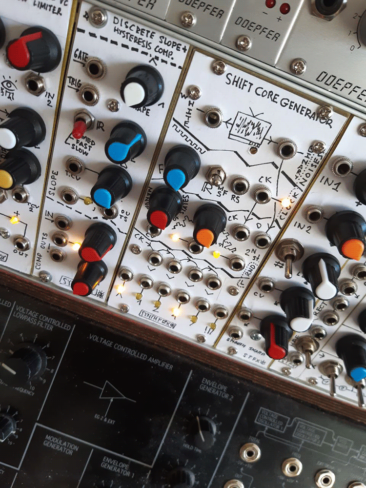
Pictures