About
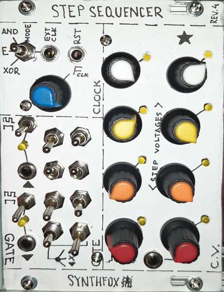
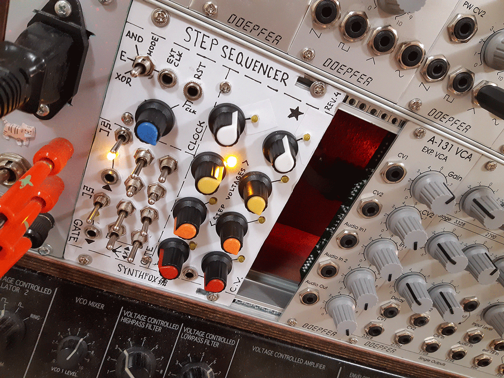
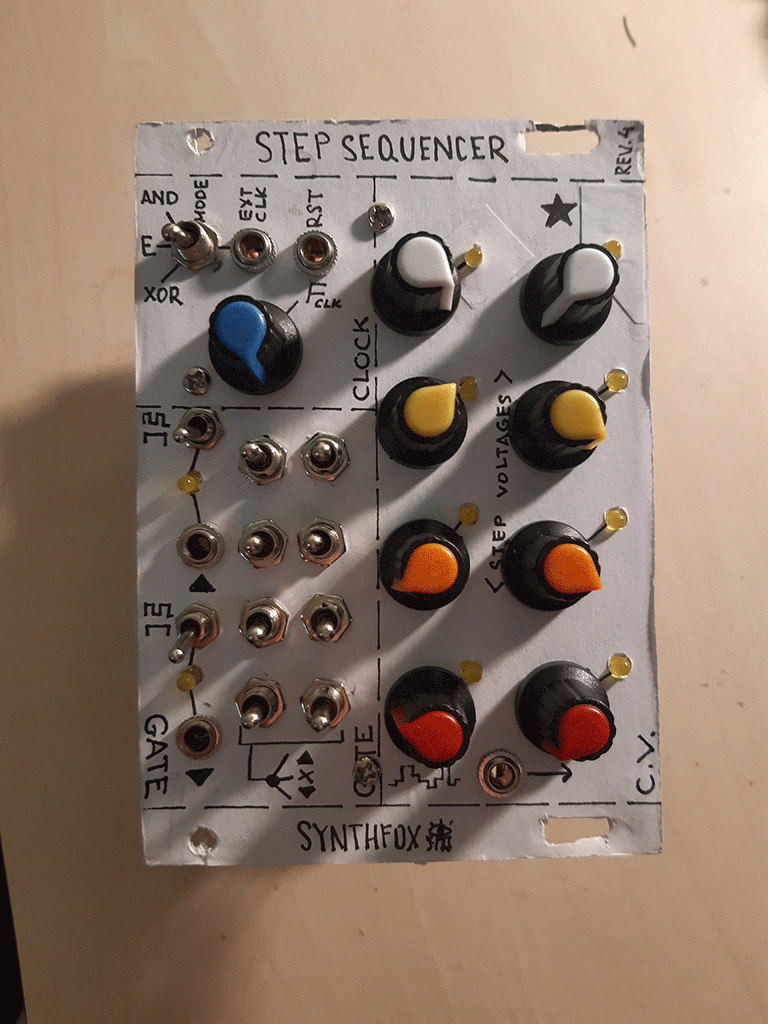
Well, this one is what it says on the cover: an eight-step sequence programmer! The reason i'm not calling it just a "sequencer" or "baby sequencer" (the popular name for 4017-based stuff) is because it has rather full sequencing capabilities: while still built on top of the good old CD4017 decade counter, it features a CV programming part and a gate programming part with tri-state step switches that drives two different gate outputs. It also has a built-in simple clock pulse generator. There's external clock and reset inputs, both with input comparators, hence are OK with sinewaves, noises and all other sorts of non-squarewaves. So, while being relatively simple, this is a complete sequence programming unit!
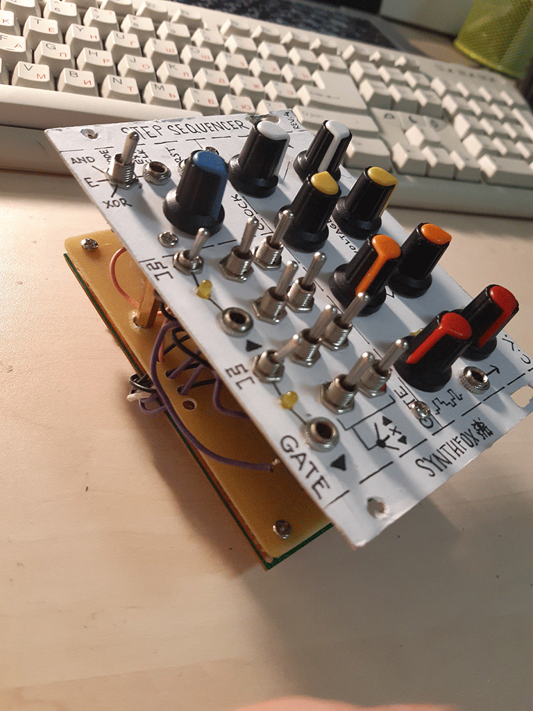
In fact, this unit has been made only because i found an old panel of the second module i ever built successfully, an 8-step sequencer. While being the same big, it didn't feature external clock or reset inputs, instead of the gate programming switches there were individual per-step gate outputs - and they weren't working. The project itself was long ago salvaged for parts, the board is somewhere in the Project Graveyard box, but the faceplate popped up while i was tidying my room, so i decided to revive this little thing to a more powerful format, and trash paperface styled, as my recent modules are.
Regarding the gate programming: some people find this one kind of complicated, so i should explain how it works. Each step has an associated switch that can either go up, down, or rest in the middle. Then, there are two gate outputs, labelled with little up and down arrows. If a step that is currently active has a switch in the up position, the gate is output from the 'up' gate out (lane1), if it is in the bottom position - the gate goes out of the 'bottom' out, and - as you might've guessed - if the switch is in the middle, there's no gate at all. Additionally, there's a special switch for each outputs: it would be incorrect to call it a "gate/trigger" switch, so i'll call it a "sync to clock" switch. Imagine we have all 8 gate steps in up position. With this switch down, we will have one continuous never-ending gate for all pattern - cause each step outputs a gate just as long as it stays active. If we pull the switch up, though, the output will get ANDed with the clock signal: this means that even if the step switch is programmed to output a gate, the output will only fire as long as the clock pulse stays high. This way, we get 8 discreet steps instead of a never-ending gate in case of an "all up" pattern.
Schematic
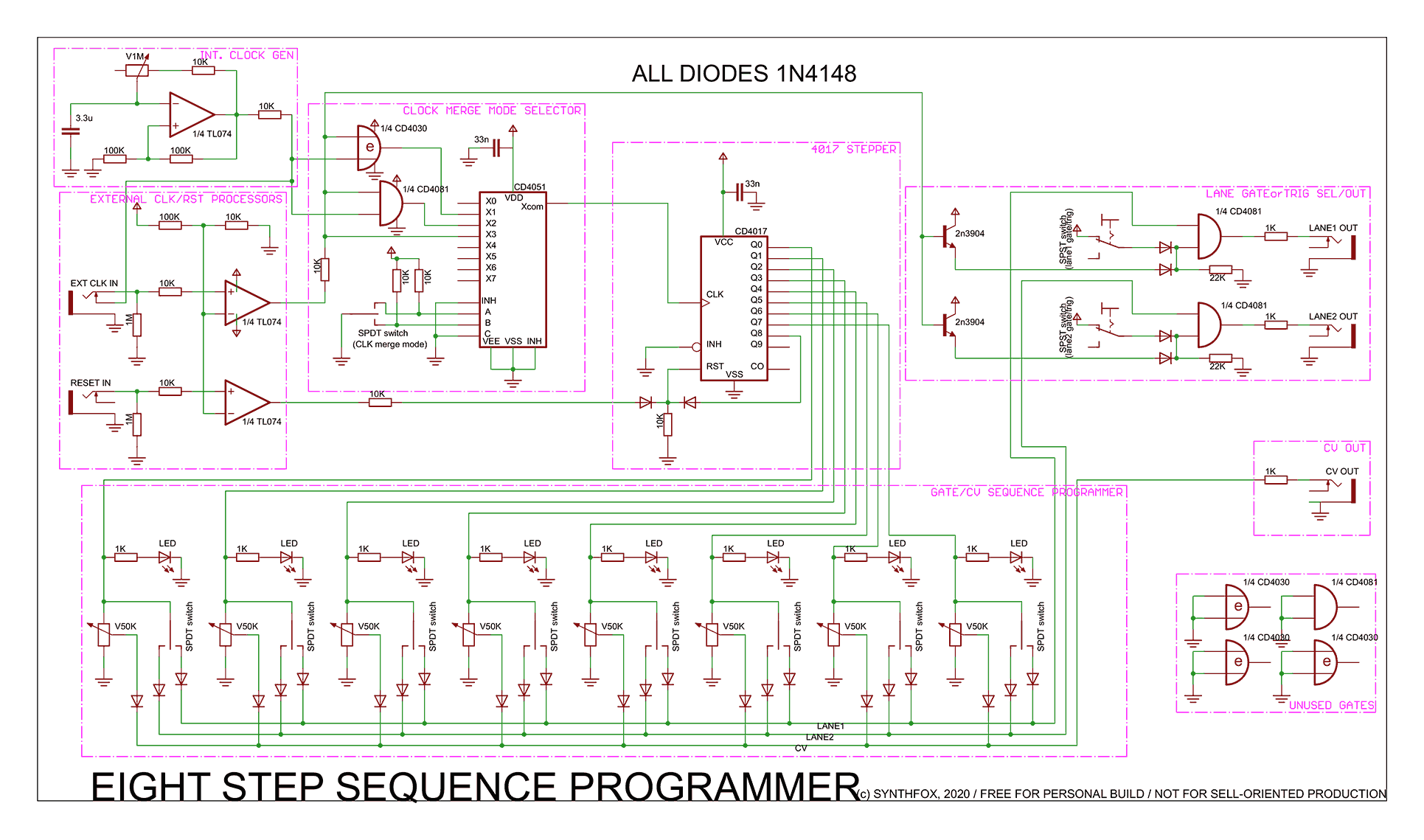
Don't be intimidated by the mean look of this one. It's actually very simple! I divided the schematic into blocks for easier understanding of what's going on, so you might want to open the image in a new tab and enlarge it.
The first block we encounter is an internal clock generator based on an op-amp: just search the web for 'op amp squarewave generator' and you'll find this exact schematic. Keep in mind that the op-amp needs to be powered from +/-12v! The squarewave output of it goes to the normalized signal of the external clock in (read: if no cable is inserted, the internal clock generator goes into the jack) and it's very important for this module to work. Also it goes to the clock merge mode selector part explained later on.
Below of the clock gen is the ext clock/reset processor (seems the block title text fell off...) and it does a very simple task: other two quarters of our TL074 (one used for clock) are set up in comparator mode and output a high voltage whenever the input goes above ~1.2 volts, and goes low when the input is below that value. This is made so that the clock and reset inputs could not only be squarewaves, but also other signals. If no clock is inserted, then the internal clock is compared to the threshold value and essentially is repeated on the output.
To the left to the clock gen and the comparators is the most tricky and most useless part of the module: the clock merge mode selector. It can easily be thrown out of the circuit, but what's the fun then? It takes in the internal and the external clock signals, and lets us clock the actual sequencer from either JUST the external clock (normalized to internal!), or the logic AND of int/ext clock, or the logic XOR of those. Why is this cool? Because you can not only drive the unit with an external pulse, but creatively merge it with the internal one! This is done very simply: logic AND and XOR are performed with the respective CMOS quad gate chips (4081 and 4030/4070), then the 4051 selector selects from either the two of those or just the external clock signal. For this, we have a dual-throw switch to ground either the A or the B pulled-up control input of the selector. In the middle position, both inputs will remove pulled up. Input C is grounded. Thus the only CAB combinations we can get are 001, 011 and 010. Look up the datasheet and you realize those are inputs 1, 2 and 3: just one of those will be selected and output to Xcom for further actions.
To the right is the simple part: just your obvious 4017 decade counter driven by the clock selected in the previous stage. The reset pin is pulled-down and there are two diode-OR'd signals going into it: step number 8 (output Q7 of 4017!) to reset the coutner automatically once 8 steps have passed, and the comparator'd external reset signal. The gates go to the gate/cv sequence programmer block below.
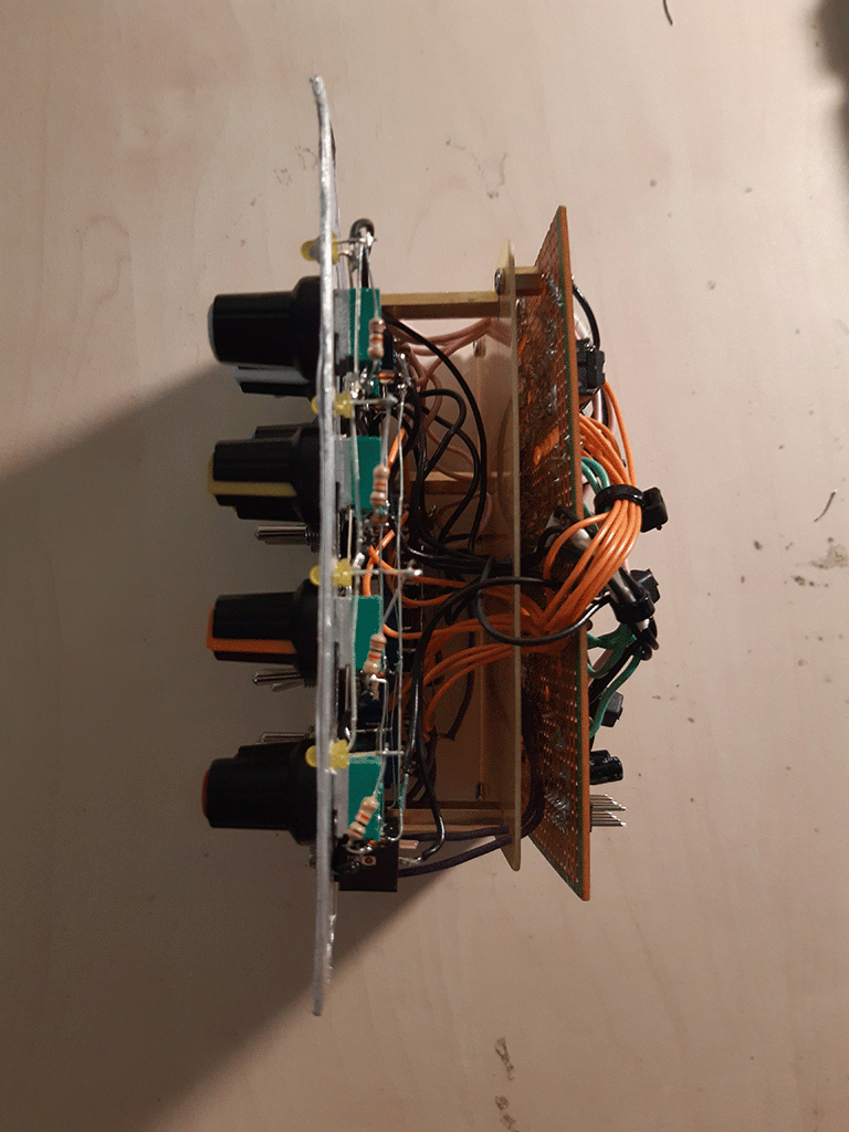
On the lowest block, the actual programming happens. We have each gate from 4017 going to the same stage: a voltage-dividing potentiometer that is then diode-mixed with all other dividers of other steps, and a dual-throw switch - with both sides diod-or'd with all other switches' sides. An inprovement could be made here: put the diodes BEFORE the switch, and not after - and save up whole 8 diodes. You can just solder the switches together, will work fine - but i'm just showing the way i did it here. The outputs of this part are the CV sequence and the gate lanes lane1 and lane2 representing up and down-set switches.
To the left of the programmer, there are two small blocks; one explicitly shows that you -should- ground all unused logic gate inputs, otherwise the circuit will wibble-wobble all over the place. The other is just an output impedance of 1K + outptut jack for the CV sequence.
A slightly harder to understand thing happens above, at the LANE GATEorTRIG SEL/OUT block. What it does is simply performs a logic AND of a lane and either the clock or a contant unchanging 1. Two quarters of the CD4081 are used for this, one per lane (another quarter used for merging int/ext clocks). One input of the gate is the lane itself: the other is a diode OR of the external clock and a switch that either outputs +12V or floats in the air. As a result, the switch either 'overrides' the clock and keeps the AND acting like a simple repeater for the lane sequence, or let the clock act and 'chop up' the lane to have separate gate for each step. A transistor buffer had to be attached to the clock source to distribute it to both ORs separately: otherwise they affect each other and the switches mess everything up. BIG NOTICE HERE: I was stupid enough to wire up the external clock as a gate source, and not the output of the selector. If you want to have a better experience, CHANGE THE SOURCE OF THE CLOCK TO THE 4051 SELECTOR OUT! The reason i'm keeping it this way here is because i already did it this way, and am keeping myself some room for actual non-theoretical improvements.
Generally, this schem is not perfect; there is a bunch of things i could either optimise, or do more interestingly, but i was accomodating for the already-existing faceplate and also i'm not that smart to actually do things the correct way, ok? A better, more featured version of such sequencer is coming someday, probably, maybe. Some hints for enthusiasts though: CVable gate mode with the remaining XORs as gateable ivertor/repeater action blocks, or use them instead of the transistors to buffer the clock. More merging modes? Gateable merged mode with XORs? Limit is fantasy!
Media
Playing a little ovbious pattern sequenced only with this unit and an external clock generator. Notice how the hits sometimes are double and sometimes are not - that's me switching the sync-to-clock gate mode switches on gate lane1 and lane2.
Same pattern as above, but now i flick the switch to demonstrate the AND of the external and internal clocks (notice the stuttering!) and then the XOR of them... which, honestly, feels a bit weird and doesn't work the way i expected it to. But should be fine! Tell me what are your experiences if you build this module.
CV for A-110/110/131 FM pair pitch, lane2 gating the A-140 envelope (it's controlling the fm depth) and lane1 to module's own RESET IN. No external clock, click merge mode set to external only - gets normalized to internal. By flicking the switches i can get different length of the sequence and different envelope triggering patterns!
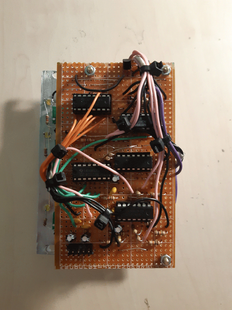
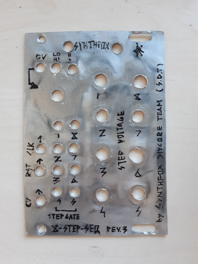
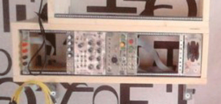
Pictures